
 Email: sales@slxytech.com
 WhatsApp / Wechat:8617062388866
 Phone:+86 17062388866
Description
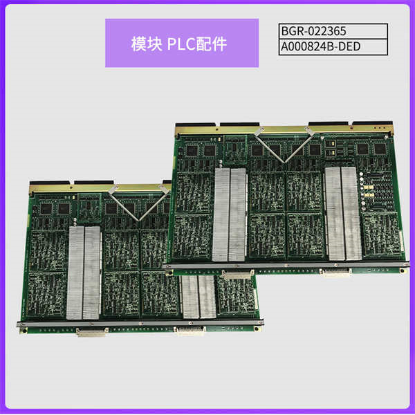
The ADVANTEST BGR-022365-A000824B-DED is a precision Device Interface Board (DIB) designed for Advantest’s high-performance semiconductor test systems, enabling nanoscale measurement accuracy in wafer-level and final test applications. This advanced interface board provides signal routing and conditioning between ATE (Automated Test Equipment) instruments and semiconductor devices under test (DUTs), supporting up to 1024 I/O channels with <0>BGR-022365-A000824B-DED integrates impedance-matched transmission lines, active thermal compensation, and embedded self-diagnostic circuits to ensure signal integrity at data rates exceeding 12.8 Gbps.
Optimized for RF/mmWave testing, the board features proprietary loss compensation technology maintaining VSWR <1>ADVANTEST DIB incorporates gold-plated spring probes and ceramic substrates to minimize signal distortion during high-volume production testing of 5G RFICs, AI accelerators, and automotive MCUs. Advanced heat dissipation channels maintain DUT temperatures within ±0.5°C during burn-in operations, significantly improving test correlation across temperature extremes (-55°C to +175°C).
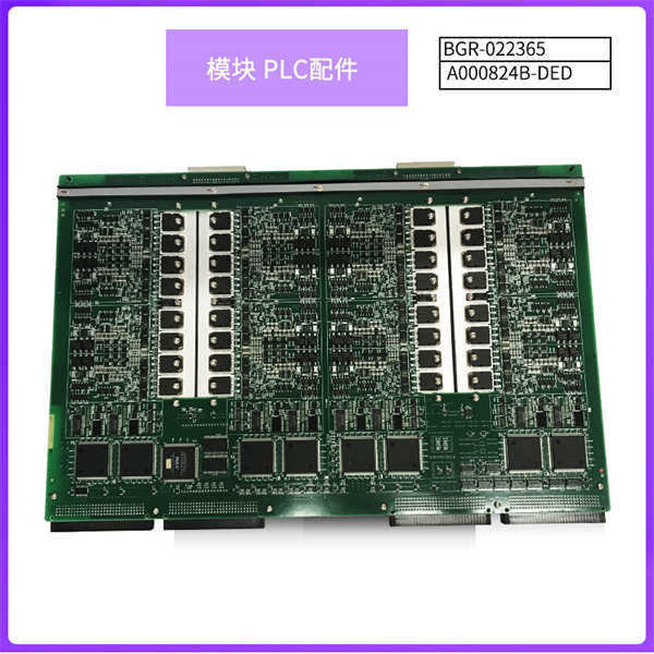
ADVANTEST BGR-022365-A000824B-DED
Technical Specifications
| Parameter Name | Parameter Value |
| Product Model | BGR-022365-A000824B-DED |
| Manufacturer | Advantest |
| Product Type | Device Interface Board (DIB) |
| Max Channels | 1024 (expandable via stacking) |
| Contact Resistance | <0> |
| Frequency Range | DC to 70 GHz (calibrated) |
| Data Rate | 12.8 Gbps (NRZ) / 25.6 Gbps (PAM4) |
| Insertion Loss | <0> |
| Voltage Isolation | 500V channel-to-ground |
| Thermal Stability | ±0.5°C (with active cooling) |
| Contactor Interface | Pogo pin / MEMS socket compatible |
| Substrate Material | Rogers 4350B / Arlon AD410 |
| Compliance | JEDEC JESD371, SEMI G85 |
Main Features and Advantages
Signal fidelity preservation: The ADVANTEST BGR-022365-A000824B-DED employs electromagnetic field simulation-optimized trace routing with cavity resonance suppression. Integrated de-embedding structures remove fixture parasitics for accurate S-parameter measurements. Active impedance tuning compensates for contactor variations during multi-site testing.
High-density scalability: Modular zone architecture enables independent channel banks for parallel testing. Each 128-channel block features localized power conditioning with <10mV>BGR-022365-A000824B-DED supports “hot-swap” site reconfiguration without system reboot, reducing changeover time by 70% during mixed-product testing.
Reliability engineering: Gold-nickel dual-layer contact surfaces withstand >1 million actuations. Embedded piezoelectric sensors detect contact force anomalies before test initiation. Proprietary thermal expansion compensation maintains positional accuracy within 3μm across operating temperatures. The board’s symmetric grounding topology achieves 80dB crosstalk suppression at 50GHz.
Application Field
The ADVANTEST BGR-022365-A000824B-DED enables advanced characterization and production testing of leading-edge semiconductors. For 5G/6G RF front-end modules, it performs load-pull measurements and EVM validation up to mmWave frequencies. AI/GPU manufacturers leverage its high parallelism for simultaneous multi-die testing of 3D-IC packages.
Automotive IC suppliers utilize the BGR-022365-A000824B-DED for AEC-Q100 Grade 0 qualification (-40°C to +150°C) with temperature-cycled parametric testing. In MEMS sensor production, it interfaces with delicate wafer-level packages using low-force contactors (<5g>
Related Products
ADVANTEST T2000-IPS: Integrated power supply for DIB auxiliary rails
ADVANTEST BGR-018740-C000512A-RF: RF-optimized DIB for 110GHz applications
ADVANTEST TS9000-MMU: Multi-site handler interface module
ADVANTEST SC1812A: Signal integrity calibration substrate
ADVANTEST V93000-SMU8: 8-channel parametric measurement unit
ADVANTEST CT1100: Contactor interface alignment fixture
ADVANTEST T6371: Thermal forcing system integration kit
ADVANTEST BGR-PDK-04: Probe development kit for wafer-level validation
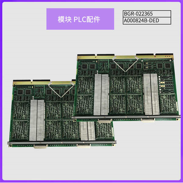
ADVANTEST BGR-022365-A000824B-DED
Installation and Maintenance
Pre-installation preparation: Verify cleanroom conditions (ISO Class 5) and ESD protocols (wrist strap <1M>ADVANTEST BGR-022365-A000824B-DED, initialize thermal calibration with vacuum chuck engaged. Pre-burn-in the board at 85°C for 24 hours to stabilize material properties.
Maintenance recommendations: Weekly clean contactor surfaces with non-residue solvent (Advantest P/N CL-77). Quarterly verify channel resistance using certified micro-ohmmeter. Replace pogo pin assemblies after 500k cycles. For the BGR-022365-A000824B-DED, perform S-parameter recalibration every 6 months using NIST-traceable standards. Store in nitrogen-purged cabinet during extended downtime.